
Apr 16
2015
2015
CI20: The DDR odyssey, part 3: memory remapping
This post is part of the CI20 bare-metal project (link leads to index of all posts), and is part three of four posts about initialising the DDR on the CI20 Creator.
In the last post we got the RAM working enough to boot something into kseg0, but we missed one curious part of RAM initialisation: memory remapping.
The jz4780 DDR controller has a several DREMAP registers, described a little opaquely as "DREMAP1~5 are used to define address mapping in DDRC.” Fine, but what is “address mapping in the DDRC”?
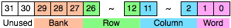
My understanding, which is basically guesswork, goes like this: We know that DDR memory addresses are specified in four dimensions: bank, row, column, and byte number within the word*. But of course physical memory addresses are a single number. So one thing you could do is just assign the various dimensions to bits within a 32-bit address space, like this:
Then physical address 0x00000000 maps to bank 0, row 0, column 0, byte 0; and physical address, say, 0x1CE1CEBB maps to bank 3, row 19996, column 942, and byte 3. (The two unused bits at the top are because we have a 4 gigabyte address space, but only 1 gigabyte of RAM to play with.)
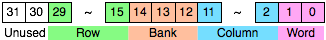
The problem with this particular mapping is that we don’t expect the bank to change very frequently. Programs tend to follow the principle of locality, which means that their next memory reference is likely to be very near their last memory reference. But DDR RAM works by “precharging” a bank + row combination, after which columns can be read. This precharging takes time, and only one row can be precharged per bank. If all the addresses we need in the near future reside in same bank but in different rows, we have no choice but to wait for the bank precharge multiple times in sequence, once for each row. If, however, the upcoming addresses span multiple banks, we could precharge all the banks we needed at once, saving some time.
In other words, we might prefer this arrangement, in which bank number should change more frequently than row number:
This is the purpose of the DREMAP registers — they let us swap bits around, effectively allowing us to change the positioning of our 4d-to-1d mapping.
And this is what the reference code (and, now, ddr.py) does: switch bank and row addresses to make it more likely that we’ll be able to precharge multiple banks simultaneously. This is actually a power / performance trade-off: we end up using more power (for bank precharging) but don’t spent so much time waiting.
Code is available under the ddr_remap tag:
If you build and run it, you should find that nothing has changed, and everything still works. Which is a comfort.
In the next post, we’ll finish off the RAM stuff by running a proper memory test.
* It’s actually five, as we also have rank, but there’s only one of those on the CI20 (ranks make more sense for removable memory, where you can define a rank as “whatever goes in a memory slot”).